


Introduction
Precision engineering in the realm of optical device production demands a meticulous alignment between design intent and manufacturing processes. Achieving the highest quality and functionality in optical devices requires a comprehensive approach that navigates through intricate design principles and precise manufacturing methodologies. This article explores the crucial steps to seamlessly align design intent with the production of optical devices.
Understanding Design Intent
Designing optical devices begins with a clear comprehension of the intended purpose, functionality, and performance expectations. Whether it’s lenses, cameras, microscopes, or telescopes, defining the design intent sets the trajectory for subsequent stages.
Specification Definition: Establishing specific parameters like focal length, magnification, resolution, and spectral characteristics forms the blueprint for the design process.
Conceptualization: Ideation and conceptualization involve brainstorming various design possibilities, considering materials, optics configurations, and manufacturing feasibility.
Bridging Design and Manufacturing
The successful translation of design concepts into tangible, high-precision optical devices hinges on effectively bridging the gap between design and manufacturing. This transition involves critical steps:
Simulation and Prototyping: Leveraging advanced simulation software aids in predicting optical performance. Prototyping allows for practical validation of the design’s feasibility and performance.
Material Selection and Characterization: Identifying the ideal materials with precise optical properties is pivotal. In-depth material characterization ensures the selected components meet design specifications.
Integrating Precision Manufacturing Techniques
The actualization of precise optical devices heavily relies on advanced manufacturing techniques synchronized with design requirements:
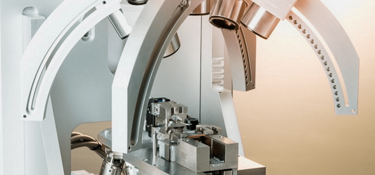
Advanced Machining and Polishing: Employing state-of-the-art CNC machining and ultra-precision polishing techniques ensures the intricate surfaces of optical components meet exact specifications.
Metrology and Quality Control: Incorporating high-precision metrology tools and rigorous quality control processes guarantees that manufactured components adhere to the intended design with minimal deviations.
Iterative Refinement and Testing
Iterative refinement is crucial for achieving optimal design-to-production alignment:
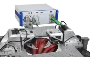
Optical Testing and Analysis: Rigorous testing utilizing interferometry, MTF (Modulation Transfer Function), and other optical evaluation methods ensures that the device meets performance standards.
Feedback Loop Integration: Implementing a feedback loop mechanism between design and manufacturing helps address any discrepancies and refine subsequent iterations for enhanced precision.
Continuous Improvement and Innovation
The pursuit of precision engineering in optical devices is an ongoing endeavor:
Adaptive Design Strategies: Embracing flexible design strategies accommodates advancements in materials and manufacturing technologies, allowing for continuous improvement.
Innovation and Research: Constant exploration of cutting-edge technologies and research endeavors fuels innovation, driving the evolution of precision engineering in optical device production.
Conclusion
The alignment of design intent with optical device production is a multidimensional process that demands meticulous attention to detail, seamless integration of design and manufacturing, and a relentless pursuit of perfection. The synergy between these steps not only ensures the realization of precise optical devices but also paves the way for innovation and advancement in the field of precision engineering. By adhering to these key steps and continuously refining the design-to-production alignment process, engineers and manufacturers can propel the evolution of optical devices, unlocking new frontiers in precision and functionality.